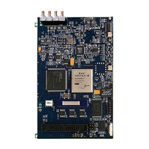
Model 474DM Tunable PCM Bit Synchronizer Mezzanine
  • Compact “mezzanine” design
  • Best-in-class noise performance
  • Fast Sync Acquisition
  • Processes all IRIG Codes
  • Data Quality and Signal Test:
    1. BERT / PRN BER Link Test Mode
    2. Frame Sync PCM BER Monitor
    3. Frame Lock/Loss Monitor
    4. Eb/No Signal Quality Output
    5. Viterbi Error Monitor / Stats
    6. Data Simulator/Generator

The 474DM Advanced Digital PCM Bit Sync is a state-of-the-art compact “mezzanine” design that provides a cost effective and modular high quality bit sync add-on to Acroamatics entire line of single slot PCI single card TM processing card products. The 474DM is compatible with both existing legacy and our latest leading-edge design telemetry card components. Based on our latest (3rd generation) bit sync design, it shares the latest techniques in FIR filtering,digital phase-locked loop, NCO clock reconstruction, and digital amplitude and offset control with it’s larger PCI cousin, the Model 1611P. Incorporating a leading-edge FPGA, the modern design delivers a greatly reduced parts count, improved reliability, and expanded capabilities – including options normally found only in box level and multi-card bit sync/encoder designs. The 474DM supports options such as Frame Sync Pattern Verification, BERT, PRN and programmable PCM simulator, and Convolutional encode/decode.

SIGNAL INPUTS (Per Bit Sync)


Source
Two (2) Inputs, Operator Program selectable
Isolation
Greater than 60dB at 20MHz
Impedance
Program selectable: Hi-Z/Lo-Z, Single Ended: 4kΩ /75Ω (std) or differential: 150 Ohm or Hi-Z (opt)
Signal Level
Single Ended: 0.2 to 20V p-p, Differential: 0.2 to 10V P-P (optional)
DC Offset
20V max Single-Ended, Hi-Z or 15V Max @ 75Ω
Baseline Variation
Tracks sinusoidal offsets to 100% p-p signal amplitude at 0.1% bit rate
PCM Codes
Program selectable: NRZ-L/M/S, Biø-L/M/S, DBiø-M/S, DM-M/S, MDM-M/S, RZ
Derandomizer
Program selectable: RNRZ 9/11/15/17/23, forward/reverse


SYNCHRONIZATION


Bit Rate Range
8bps to 40MHz, all PCM Codes
Tuning Resolution
0.1% of bit rate
Capture Range
3 times the programmed loopwidth, typical
Tracking Range
±12% typical, with programmable limiter
Loop Bandwidth
0.1% to 3.2%, program selectable in 0.1% increments
Sync Threshold
0db for NRZ-L and Biø-L codes
Sync Acquisition
(LW=1.6%, SNR > 12dB) Typically less than 50 bit periods
Sync Retention
(LW=0.1%, SNR > 3dB) Retains sync through > 1024 consecutive dropouts
Bit Error Rate
(LW=0.1%) to within .50 dB of ideal bit error rate performance curves


DATA/CLOCK OUTPUTS, NRZ-L


NRZ-L Data
One each, NRZ-L data/clock pair, RS422/TTL (jumper selectable) – operator program output selectable to INTERNAL (direct to host decom card via internet bus) or EXTERNAL (output pair directed to card external output BNC or Triax cables)
Data Clock
0°, 90°, 180°, 270°, operator program selectable
Data Polarity
Program selectable: normal/inverted


DATA/CLOCK OUTPUTS, CODE (Dual PCM Encoders)


Data Source
Program selectable: Recovered Data (Bit Sync NRZ-L Data/Clock – DEFAULT) or External Data/Clock (PROGRAM SELECTABLE).Three each: One each TTL data/clock (0° & 180° selectable) Code (selectable) PCM and Clock, One each TTL data RNRZL, One each TAPE (code selectable) TTL or ±2 Volts balanced output, 50mA drive current.
Randomizer
Program selectable: RNRZ 9/11/15/17/23, forward/reverse
PCM Codes
Program selectable: NRZ-L/M/S, Biø-L//M/S, DBiø-M/S, DM-M/S, MDM-M/S, RZ


EXTERNAL DATA/CLOCK PCM ENCODER INPUT


Signal Type
Jumper selectable: RS-422 or TTL
Impedence
120Ω , RS-422, 75Ω TTL
Data Code
Program selectable: NRZ-L/M/S, Biø-L/M/S, DBiø-M/S, DM-M/S, MDM-M/S, RZ
Data Clock
Program selectable: Normal/Inverted, 1x or 2x


CONVOLUTION ENCODER/DECODER (Optional)


Viterbi Decoder
Rate 1/2, k=7: includes differential decoding, V.35 descrambling, and G2 invert (others available)
Symbol Formats
Serial, parallel, and staggered parallel (others available)
Convolution Encoder
Rate 1/2, k=7: includes differential encoder, V.35 scrambler, and G2 inverter (others available)
Symbol Formats
Serial, parallel, and staggered parallel (others available)


FORMAT GENERATORS/SYNCHRONIZER (Optional)


Format Generator
Programmable frame length, sync pattern and mask
Synchronizer Source
Recovered data, external data or test generator
Synchronizer Strategy
Pattern match in “search”, programmable error limits for “check” and “lock” states
Other Features
Bit slip enable, auto polarity enable, data source/ambiguity resolution


BIT ERROR RATE TESTER (Optional)


Transmitter Pattern
PRN sequence: PN7, PN9, PN11, PN15 (forward/reverse)
Pattern Clock Source
Program selectable: Bit Rate Clock or External Clock
Blanking
Program selectable: 64, 128, 256 bits
BER Sample Period
Program selectable: 1E3 to 1E9 bit periods, or continuous accumulate
Variable Output
50mV to 5V P-P
Other Features
Automatic pattern sychronization, forced error ON/OFF


PHYSICAL


Hosts Supported
Plugs onto Models 1611P, 1626P, 1612P, & 1622P (PCI) and Legacy 1601P, 1602P (PCI) & 1502V (VME) cards, & RS-232
Cooling Requirements
30 Linear FPM
Power Requirements
+5VDC @ 1.25A, ±12VDC @ 0.25A
Dimensions
6.5″ (16.51cm) H x 4.0″ (310.16cm) W x .625″ (1.5875cm) D
Temperature
Operating: 0° to +40° C, Non-operating -40° to 86° C
Relative Humidity
Up to 90% non-condensing
Shock
Operating 6G, Non-operating 25G
Vibration
Operating 0.3G, 5 to 2000 Hz, Non-operating 0.8G, 5 to 500 Hz

Specifications subject to change without notice.